The STM32F103C8T6 belongs to the STM32F103 medium-density performance line, built on a high-performance Arm Cortex-M3 core running at 72 MHz. It features up to 128 KB of Flash memory, up to 20 KB of SRAM, and a wide range of I/Os and peripherals connected via two APB buses. It supports two 12-bit ADCs, three general-purpose 16-bit timers, one PWM timer, and multiple communication interfaces including two I2Cs, two SPIs, three USARTs, USB, and CAN.
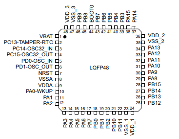
Power Supply Pins
VBAT (pin 1): Backup domain power supply.
VDD (pins 9, 36, 48): Main power supply.
VSS (pins 8, 35, 47): Ground reference.
VDDA (pin 7): Analog power supply (ADC and DAC).
VSSA (pin 6): Analog ground.
NRST (pin 7): Reset pin.
Oscillator Pins
PC14-OSC32_IN (pin 3): crystal oscillator input.
PC15-OSC32_OUT (pin 4): crystal oscillator output.
PD0-OSC_IN (pin 5): High-speed external (HSE) oscillator input.
PD1-OSC_OUT (pin 6): High-speed external (HSE) oscillator output.
Debug & Programming Pins
PA13 (SWDIO) (pin 34): Serial Wire Debug I/O.
PA14 (SWCLK) (pin 37): Serial Wire Debug Clock.
PA15 (JTDI) (pin 38): JTAG Data In.
PB3 (JTDO) (pin 39): JTAG Data Out.
PB4 (JNTRST) (pin 40): JTAG Reset.
GPIO and Peripheral Pins
Port A (PA0 - PA15): Pins 10 to 15, 28 to 38.
Port B (PB0 - PB15): Pins 18 to 27, 39 to 46.
Port C (PC13 - PC15): Pins 2 to 4.
Port D (PD0 - PD1): Pins 5 and 6.


| Specification | Details |
| Core | 32-Bit Single-Core |
| Number of I/O | 37 |
| Speed | 72 MHz |
| Flash Memory | 64 KB |
| SRAM | 20K x 8 |
| Supply Voltage | 2V ~ 3.6V |
| Temperature Range | -40°C ~ 85°C |
| Data Converters | A/D 10x12b |
| Package Types | 48-LQFP |
Arm® 32-bit Cortex®-M3 CPU core
Single-cycle multiplication and hardware division
PLL for CPU clock
Sleep, Stop and Standby modes
VBAT supply for RTC and backup registers
Dual-sample and hold capability
Temperature sensor
Peripherals supported: timers, ADC, SPIs, I2Cs and USARTs
4 IC/OC/PWM or pulse counter and quadrature (incremental) encoder input
Motor drives
Industrial control systems
Medical and handheld devices
PC peripherals and gaming accessories
GPS modules
Programmable logic controllers (PLCs)
Inverters and power control
Printers and scanners
Alarm and security systems
Video intercom systems
HVAC control systems
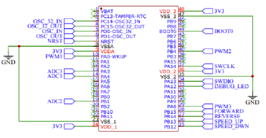
This circuit diagram shows the core peripheral connections of the STM32F103C8T6 chip. The power supply of the chip is powered by multiple 3.3V power pins (3V3); the ground pin (GND) of the chip is connected to the common ground of the circuit. The clock part uses an external crystal oscillator circuit (OSC32_IN, OSC32_OUT, OSC_IN, OSC_OUT) for clock signal input.
The I/O port part (such as PA0-PA15, PB0-PB15) is assigned to different functional interfaces, including PWM output, ADC sampling and general GPIO functions. PWM1, PWM2, and PWM3 correspond to different control signal outputs. The debugging and programming interface uses SWDIO and SWCLK signals. In addition, the circuit also includes common functional designs such as BOOT0 pin selection and debug LED indication to facilitate software debugging and hardware status indication.
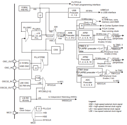
This clock tree diagram illustrates the complete clock structure of the STM32F103C8T6 microcontroller. The MCU integrates multiple clock sources, including the high-speed internal RC oscillator (HSI), high-speed external crystal oscillator (HSE), low-speed internal RC oscillator (LSI), and low-speed external crystal oscillator (LSE).
The PLL (Phase-Locked Loop) is a crucial module that multiplies the input HSE or HSI clock signal to achieve a higher system clock frequency. The PLL's output, PLLCLK, is divided to generate the system clock SYSCLK. This system clock is then distributed via AHB, APB1, and APB2 prescalers to create different bus clocks: HCLK, PCLK1, and PCLK2. These bus clocks provide appropriate clock speeds for different peripherals. For example, the APB1 bus can provide a suitable clock frequency for low-speed peripherals, while APB2 can provide a faster clock signal for high-speed peripherals.
Datasheet PDF(https://dir.heisener.com/DatasheetDownload/STM32F103VBT7TR.pdf)
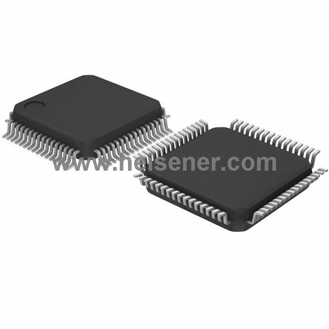
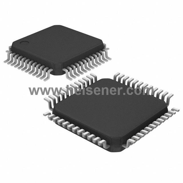
STM32F103C8T6 comes in LQFP package, which is a 48-pin, 7 x 7 mm low-profile quad flat package, featuring a 0.5 mm pitch that gets reliable connectivity while optimizing board space.

To start using the STM32F103C8T6, set up your development environment using STM32CubeIDE or Keil uVision, and configure the microcontroller with STM32CubeMX.
Then connect your board to your computer via USB, create a new project, and set up peripheral configurations like USART or SPI in the IDE. Use the HAL libraries to write your C code, then build the project to generate the binary file.
Finally, flash your code onto the chip using an ST-Link programmer, and debug it to ensure everything runs smoothly.
It’s a 32-bit microcontroller from STMicroelectronics based on the ARM Cortex-M3 core, running at 72 MHz with 64 KB flash and 20 KB SRAM.
It has 2 ADCs, 3 timers, 1 PWM timer, multiple communication interfaces (USART, I2C, SPI, CAN, USB).
Yes, you can use an ST-Link debugger for flashing and debugging in IDEs.
It’s widely used in motor drives, industrial controls, medical devices, PC peripherals, and more.